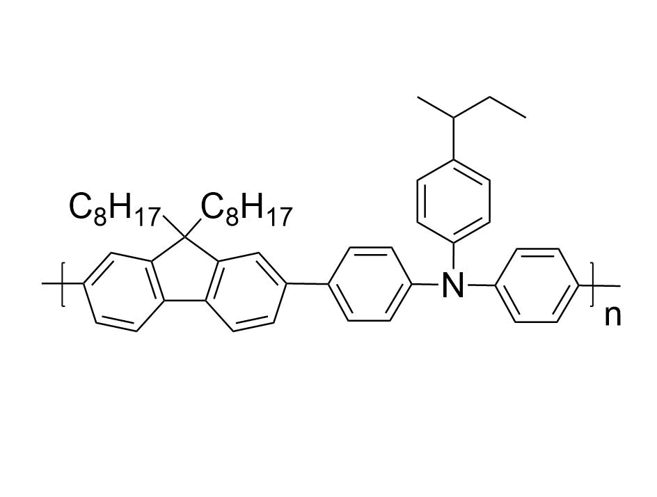
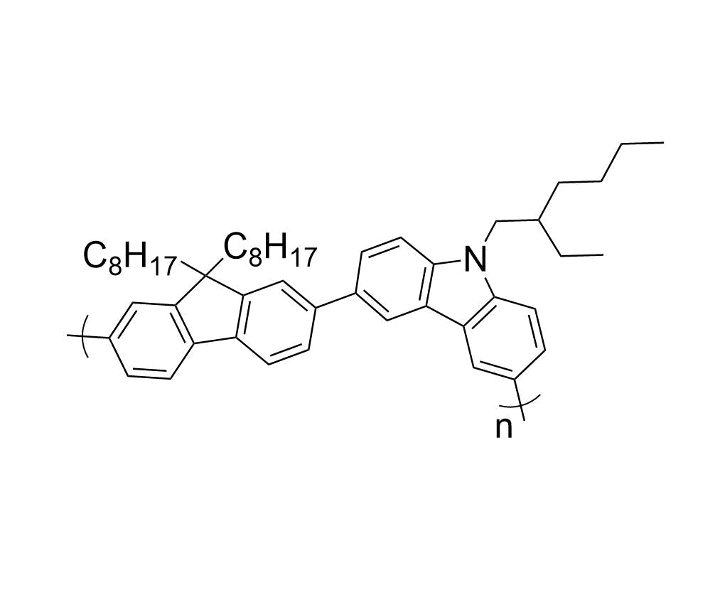
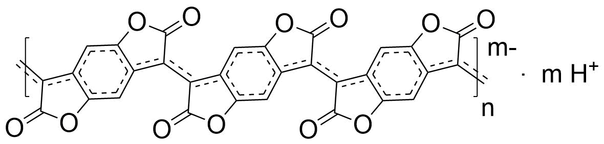
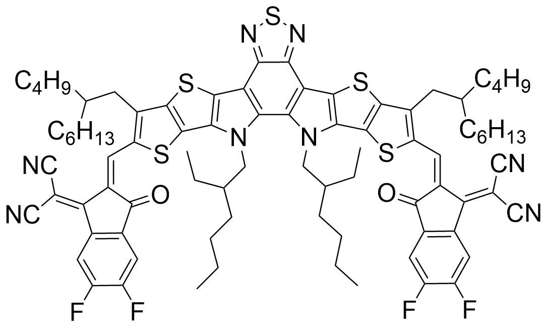
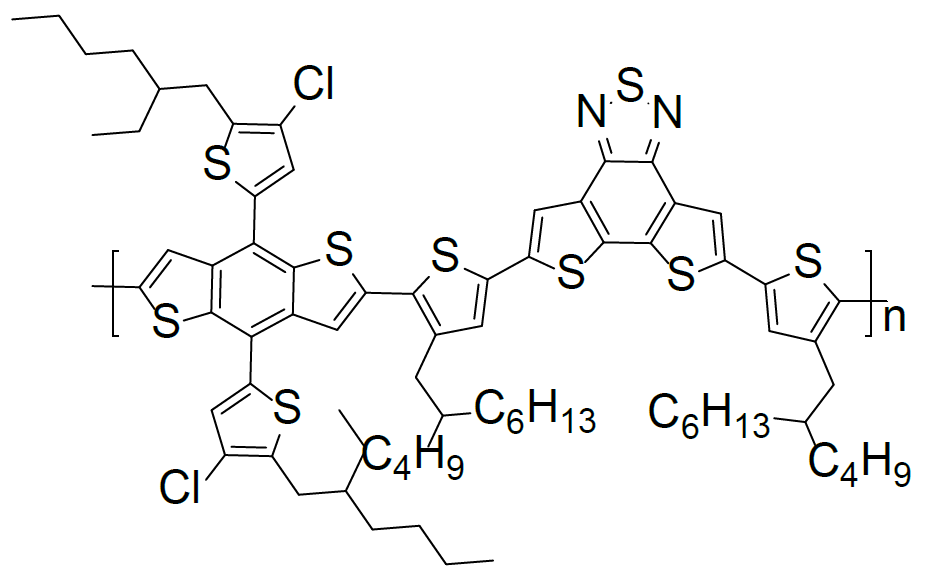
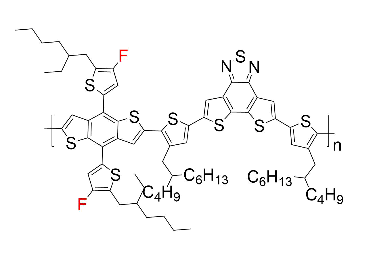
Optimizing the hole transport layer (HTL)/electron transport layer (HTL) in organic optoelectronic devices can significantly improve device efficiency, and voltammetry optoelectronics can design and develop materials according to different device types required by customers